From incoming silicon verification to 3D X-ray inspection and extreme environmental stress testing, explore the multi-layered quality control architecture that guarantees zero-defect reliability across automotive, medical, and mission-critical electronics.
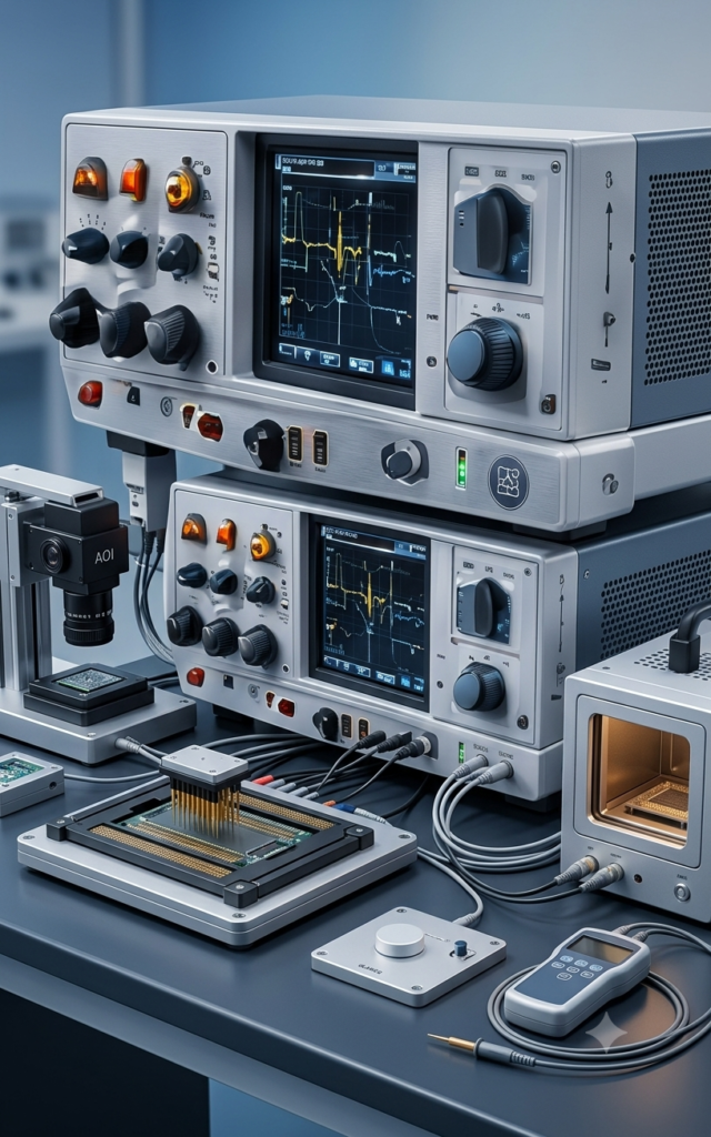
Quality isn't inspected in at the end—it is engineered into every millisecond of the fabrication and assembly cycle. Here is how Hoss Electronics safeguards every single board.
Every passive component, semiconductor, bare laminate, and solder alloy is rigorously verified before entering the clean-room production floor.
Continuous closed-loop optical and laser monitoring during solder stencil printing, component pick-and-place, and reflow soldering.
Comprehensive electrical, functional, and environmental stress validation before boards are cleaned, sealed, and packaged.
Combining high-resolution optics, deep penetrative X-ray imaging, and automated probe robotics to detect sub-micron solder defects.
Using multi-angle multi-color LED projectors and high-speed CMOS sensors, 3D AOI reconstructs topographies of every solder joint in true microscopic detail.
Non-destructive X-ray penetration is mandatory for Ball Grid Arrays (BGA), Quad Flat No-Leads (QFN), and land grid packages where joints are physically invisible to optical cameras.
Precision software-steered mechanical needles touch test pads across the board, measuring component values, tracing opens, and verifying impedance without custom tooling costs.
Custom spring-loaded bed-of-nails test fixtures press onto hundreds of test points simultaneously, diagnosing complete circuit schematics in seconds for high-volume runs.
Simulates operating conditions in the final product. We flash target firmware, inject signals, cycle relays, and read back digital bus telemetry (CAN, UART, I2C, SPI).
We expose boards to accelerated thermal cycling and mechanical vibration to trigger infant mortality failures in factory chambers rather than in the field.
Understand how each testing and inspection method fits your product lifecycle, production volume, and budget.
| Test Method | Defect Coverage | Fixture Cost | Test Speed / Board | Best Suited For |
|---|---|---|---|---|
| 3D AOI (Optical) | Component presence, polarity, solder fillets, bridges | Zero Cost | Fast (15 - 30s) | 100% of all SMT production boards |
| 3D AXI (X-Ray) | BGA voiding, hidden solder shorts, PTH barrel fill | Zero Cost | Moderate (30 - 60s) | Complex BGAs, QFNs, and multilayer boards |
| Flying Probe (FPT) | Opens, shorts, passive LCR values, diodes | Zero Cost | Slow (3 - 10 min) | Prototypes, NPI, and small batch runs (< 500 pcs) |
| ICT (Bed of Nails) | Complete electrical net analysis, component values | Moderate / High | Ultra-Fast (5 - 15s) | Mass production runs (> 1,000 pcs) |
| FCT (Functional) | Firmware, real-world logic, bus comms, sensors | Moderate (Jig) | Application Dependent | Complete turn-key assemblies & box builds |
| Burn-In Aging | Infant mortality, temperature drift, thermal breakdown | Chamber Runtime | Hours / Days | Defense, Aerospace, Medical, Automotive |
Common questions electronic engineers and sourcing managers ask about electronics testing.
IPC Class 2 covers dedicated service electronic products where continuous operation is desired but not critical (such as industrial instruments and telecommunications). IPC Class 3 is the highest standard, mandated for mission-critical electronics where downtime cannot be tolerated, including medical life-support systems, aerospace, defense, and automotive safety electronics.
BGA (Ball Grid Array) and QFN (Quad Flat No-Leads) packages have solder balls hidden completely beneath the chip body, making optical inspection (AOI) impossible. Automated 3D X-Ray penetration verifies hidden solder joint shape, detects bridging, and calculates the voiding ratio to ensure it stays below IPC's 15% to 25% threshold.
Flying Probe Testing (FPT) uses software-guided robotic needle probes with zero fixture costs, making it ideal for rapid prototypes, NPI, and low-to-medium volumes. In-Circuit Testing (ICT) requires an expensive custom bed-of-nails fixture but tests hundreds of test points simultaneously in seconds, making it the most cost-effective solution for high-volume mass production.
We enforce strict Incoming Quality Control (IQC) by procuring exclusively through authorized factory-direct distributors. Components undergo visual microscopy, marking permanence solvent tests, package X-ray examination, and Electrical LCR parameter verification prior to line stocking.
Yes, our test engineering team designs custom FCT fixtures complete with pogo-pin beds, microcontroller programming harnesses, automated sensor stimulus, and digital logging software to record pass/fail serial records for every produced unit.